Focused Ion Beam (FIB)
Focussed Ion Beam (FIB) is a microscopy technique in which a beam of ions can be used to destructively remove material through a process known as sputtering. Gallium ion dual beam systems are now widely available; these systems are well suited to TEM sample preparation, ion channelling imaging and small 3D reconstructions.
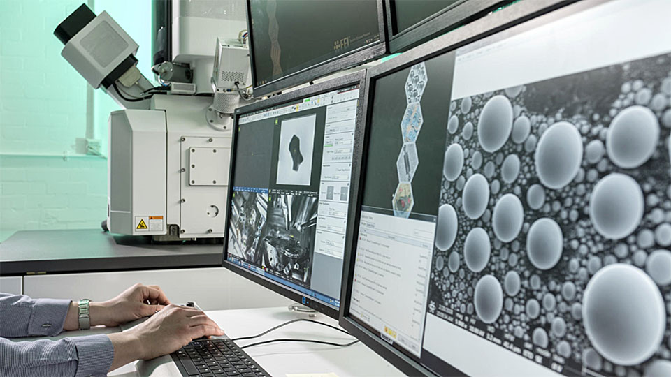
LMCC has two focussed ion beam systems one which uses a gallium ion source and another which uses a Xenon plasma. Our Xenon plasma FIB (PFIB) has revolutionised the sector - we can now produce cross sections up to 800 µm in width. This new functionality has proved invaluable to both academic researchers and clients from industry.
Typical industrial uses
Cross sections
- Paint defects
- Corrosion products
- Thickness and composition of deposited coatings
- Internal structure of powders and fibres
- Fuel cell layer thickness and composition
- Failure analysis / comparison
TEM sample preparation
- TEM sample preparation
- Bulk metals and ceramics
- Powders
- Site specific lift outs
- Crystal orientation specific lift outs for dislocation and precipitate analysis
In situ STEM imaging
- Particle size analysis of nm scale powders
- Preliminary TEM sample screening of carbon extraction replica and electro polished samples
3D reconstructions
- Precipitate to void analysis in steels
- 3D visualisation of failure locations in electrical packaging
Key Capabilities
- 3D reconstructions (serial sectioning)
- Atom probe preparation
- Cross section analysis
- Crystal orientation specific TEM sample preparation
- Energy Dispersive Spectroscopy (EDS)
- Everhart-Thornley Secondary Electron Detector (SE)
- HD Backscattered Electron Detector (BSD)
- MEMS hot stage analysis
- TEM sample preparation
LMCC currently has two focussed ion beam (FIB) instruments, details of which can be obtained below:
FEI - Helios G4 PFIB Xe DualBeam

Built-in detectors:
- SE2 (secondary electron)
- InLens (secondary electron detector within column)
- EsB (energy-selective backscattered electron within column)
- BSD (backscattered electron, retractable)
- STEM (scanning transmission electron microscopy, retractable)
- A Gatan Monarc Pro CL system with a cooled PMT (185-980 nm) CCD (185 - 1100 nm) with an additional (900 – 1900 nm) InGaAs diode
Analytical detectors:
- OI Symmetry EBSD (electron backscatter diffraction) CMOS detector
- OI Ultim Max EDS (energy dispersive spectroscopy) detector
Gas injection system:
- Platinum
- Tungsten
- Carbon
- Xenon fluoride (enhanced silicon milling)
Cryogenic Stage:
- Gatan Cold Stage, Model C1002. Nitrogen cooled stage for SEM (-185 to +200 °C)
- Stage movement (X,Y full range, t45° R+/-25°)
Thermofisher - Scios 2 Ga DualBeam

Built-in detectors:
- SE2 (secondary electron)
- Trinity TLD (T1, T2, T3, through the lens detectors)
- BSD (backscattered electron, retractable)
Analytical detectors:
- OI Infinity 100 EDS
Gas injection system:
- Tungsten
- Xenon fluoride (enhanced silicon milling)
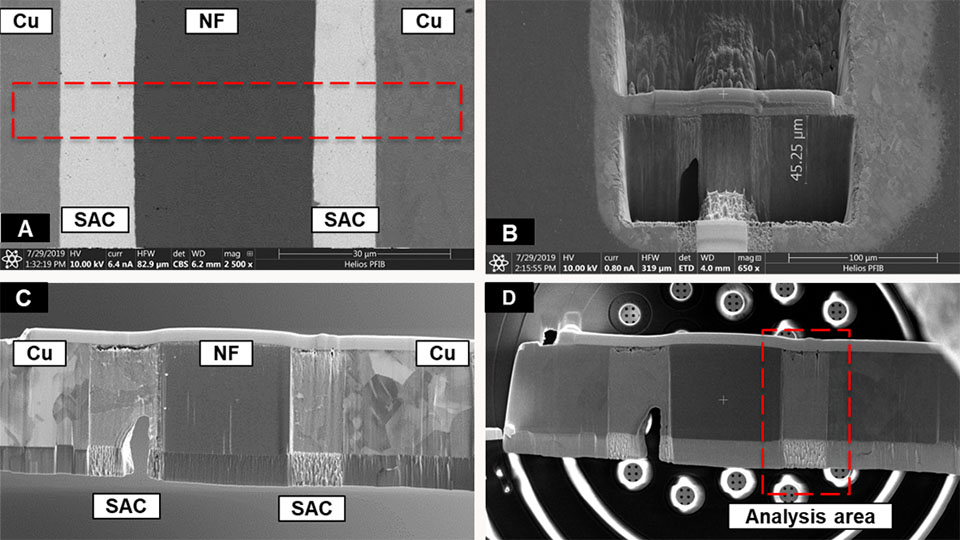
Materials have traditionally been characterised in two dimensions as polished samples. The P-FIB allows materials to be serially sectioned and reconstructed in 3D this allows the real shapes and sizes of grains or precipitated phases to be observed. In addition to this, the connectivity of features within the microstructure can be observed, which allows researchers to fully characterise materials with asymmetrical and inhomogeneous microstructures. Using the P-FIB 300 µm x 100 µm x 80 µm volumes of material can routinely be serial sections and reconstructed. This gives us the opportunity to produced data set of statistically significant volumes of material.
Case Studies
Are you interested in using this technique?
If you are interested in using this technique and would like further information please do not hesitate to get in touch.