Transmission Electron Microscopy
TEM is a microscopy technique in which a beam of electrons is transmitted through a thin specimen, interacting with the specimen as it passes through. An image is formed by detecting the scattered electrons exited the specimen to reveal its internal microstructure. TEM provides morphology and chemical composition of a solid at atomic resolution, as well as its crystal structure. As a key analytical instrument in the physical, chemical and biological sciences, TEM finds wide applications in materials science, pollution, nanotechnology and semiconductor research, as well as cancer research and virology.
Typical industrial uses
Direct imaging of microstructure up to atomic resolution
- Thin film, epitaxial layer on substrates
- Semiconductor metrology, superlattice wavelength, layer thickness
- Interface orientation relationship direct imaging
- Thickness and composition of deposited coatings
- Nanoparticles size measurement and distribution
- Al alloys precipitates hardening process
- Steels and Ni superalloys carbides distribution
Phase identification
- Selected area electron diffraction on secondary phases, precipitates
- Crystal orientation relationship by diffraction
Chemical mapping and line-scan
- Corrosion and thermal degradation, Grain boundary/interface elemental diffusion
- Chemical segregation at grain/phase boundary, elemental depletion at grain boundary
In situ TEM imaging
- Nanoparticles ripening while been heated
- Interface voids coalescence as a function of heating in vacuum
Key Capabilities
- High resolution imaging
- High resolution chemical mapping
- Secondary phases/precipitates phase identification
- Crystal orientation relationship by electron diffraction
- Interface sharpness/cleanness nanoscale imaging and elemental mapping
- Energy Dispersive X-ray Spectroscopy (EDX)
- High angle annular dark field imaging (HAADF)
- MEMS in-situ heating stage
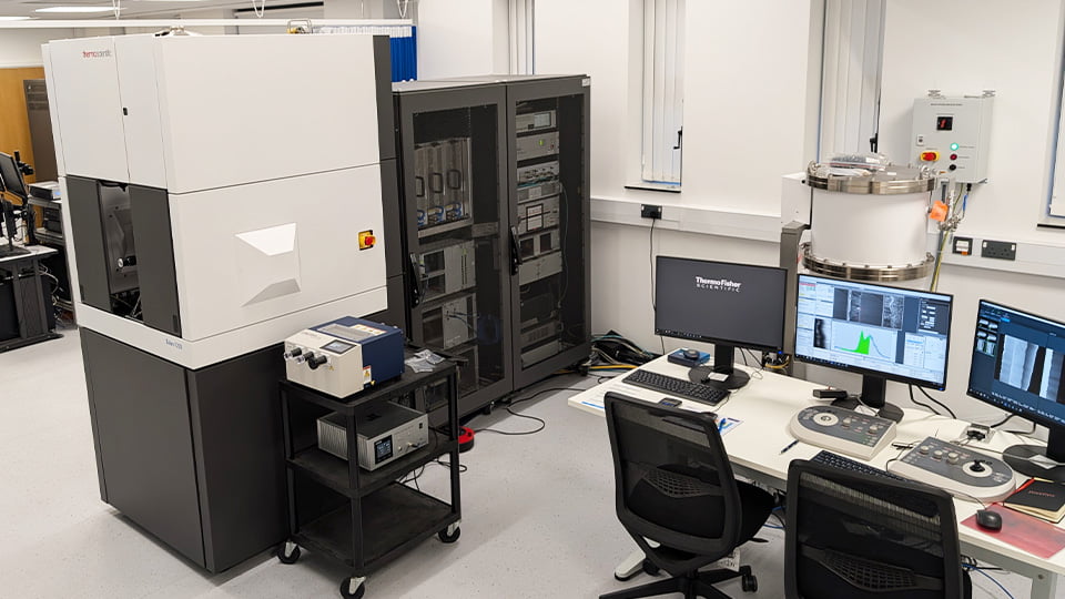
Talos F200i CFEG STEM / TEM + x2 100mm EDS detectors
- Cold FEG offering high brightness and resolution
- Alignments at 60 kV 80 kV 120 kV and 200 kV
- 2 x Bruker x Flash6 100 EDS detectors
- Ceta-S Camera, Segmented Panther STEM and 4D STEM capability
- Singe tilt holder, Melbuid Cryo holder (-155°C) , High-visibility Low-background Double-tilt Holder, MEMS based in-situ heating holder
Attolight CL system
- Detectors, PMT 200-650 nm, CCD (200-1060nm), NIR (800-1700 nm) InGaAs
- Acquisition capabilities include
- Wavelength-filtered and unfiltered CL mapping plus spectrum imaging (hyperspectral imaging).
- Sequential CL and EDS collection (with the same holder)
Are you interested in using this technique?
If you are interested in using this technique and would like further information please do not hesitate to get in touch.