Micro bending case study
In-situ micro mechanical testing
Background
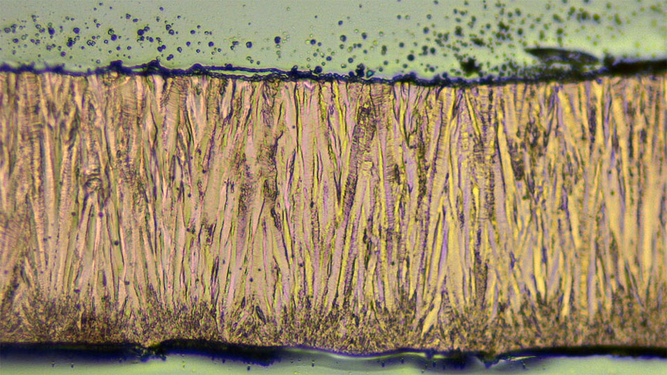
The introduction of twins is a promising method for the strengthening of copper without reducing its ductility or electrical conductivity, however, further information is required to understand the effect of nano twins on the mechanical properties of copper interconnects. Due to the fine layer thickness of electroplated copper nanotwins, micro mechanical testing is one of the only suitable techniques for accurate characterisation of bending strength.
Experimental
A FEI G4 CXe P-FIB-SEM (FEI, Oregon, USA) instrument at the Loughborough University characterisation centre was used for the preparation of the microbeam cantilevers. The technique used required a chunk lift-out onto silicon followed by ion beam milling to shape.
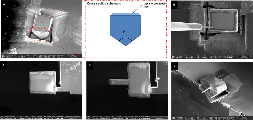
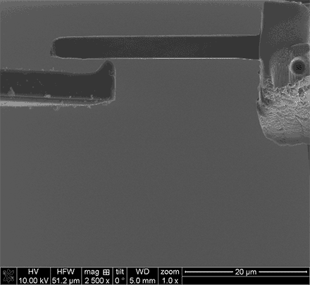
The sample was then bent in the Nova 600 with the kleindiek force measurement probe.
Results
The micro cantilever fabricated had a width of 3.45 ± 0.05 µm, height of 3.72 ± 0.15 µm and length of 25.0 µm. During testing the microbeam was found to significantly plastically deform.
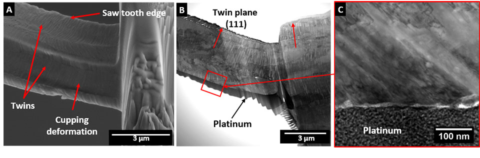 The Young’s modulus of the copper nanotwins was found to be 78.7 ± 11 GPa, (error calculated based on cross section variation.) The Young’s modulus of copper at the macro scale is widely accepted as 117 GPa, however, depending on the crystallographic orientation of individual grains, the copper’s modulus can vary from 59-77 GPa in the [001] direction up to 160-202 GPa in the [11] direction 8,17. The flow stress of the copper microbeam was calculated to be 0.80 ± 0.06 GPa based on the methodology presented by C. Motz et al. 13. The estimated flow stress of the nanotwinned copper is higher than those reported for equiaxed copper micro beams of a comparable size (3.5 × 3.5 µm) in the literature, being 0.334 GPa 13. This increase in flow stress can be attributed to the strengthening effects of the twins in the sample blocking dislocation movement; TEM analysis showed very high dislocation densities around the root of the cantilever.
Summary
Nanotwinned copper exhibited elevated flow stress when subjected to micro bending suggesting it may be a suitable candidate material for electrical interconnections.
Acknowledgement
Stuart Robertson
Funding
This research was supported by EPSRC (Grant No. EP/R032203/1) funding awarded to Professor Changqing Liu and Dr Zhaoxia Zhou
Publications / References
ROBERTSON, S., DOAK, S., SUN, F.‐L., LIU, Z.‐Q., LIU, C. and ZHOU, Z. (2020), Focused ion beam preparation of microbeams for in situ mechanical analysis of electroplated nanotwinned copper with probe type indenters. Journal of Microscopy. doi:10.1111/jmi.12868