High spatial resolution EBSD
Introduction
Electron backscatter diffraction (EBSD) has traditionally been performed at 20 kV accelerating voltage, resulting in a large interaction volume that limits its effectiveness for grain size analysis at high resolution. Lowering the accelerating voltage can reduce this interaction volume, but conventional EBSD cameras struggle with extended acquisition times at reduced voltages.
Technological Advancements
The introduction of CMOS detectors has significantly improved sensitivity, allowing EBSD patterns to be captured efficiently at 10 kV. This advancement enables the characterization of materials with sub-micron grain sizes, which previously required transmission electron microscopy (TEM) for adequate resolution.
Application Example
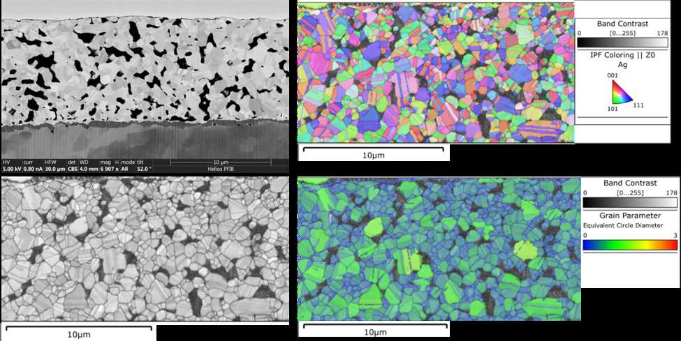
A P-FIB cross-section of a nano-silver sintered die attachment was analysed using EBSD at 10 kV with a beam current of 6.4 nA and a step size of 50 nm. The results demonstrated the capability of low-kV EBSD to resolve fine-grained structures effectively, pushing the resolution limits of the technique.
Conclusion
With improved detector sensitivity, EBSD can now provide high-resolution grain size analysis at lower accelerating voltages, bridging the gap between SEM-based and TEM-based material characterization. This advancement enhances the applicability of EBSD for analysing fine-grained materials in various industrial and research settings.
Acknowledgement
Dr Stuart Robertson