Optimizing Cathodoluminescence Analysis in Solar Cells case study
Introduction
Cathodoluminescence (CL) is an essential technique for analyzing photovoltaic materials at the nanoscale. It provides insights into band gap distribution, grain boundaries, and elemental segregation. However, preparing transmission electron microscopy (TEM) samples without damaging the CL signal is a challenge. Focused ion beam (FIB) techniques, particularly gallium (Ga) and xenon (Xe) ion milling, impact CL analysis differently. This study evaluates ion-induced damage in CdTe and presents an optimized workflow for CL-guided TEM sample preparation.
Experimental
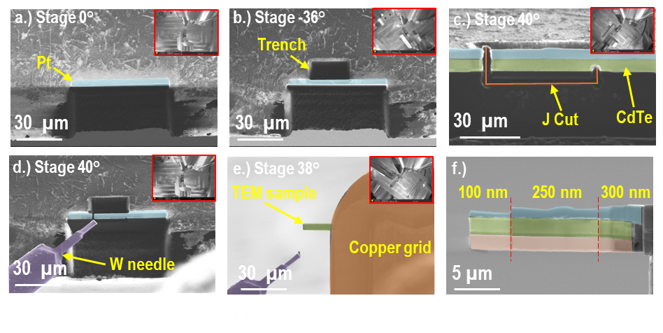
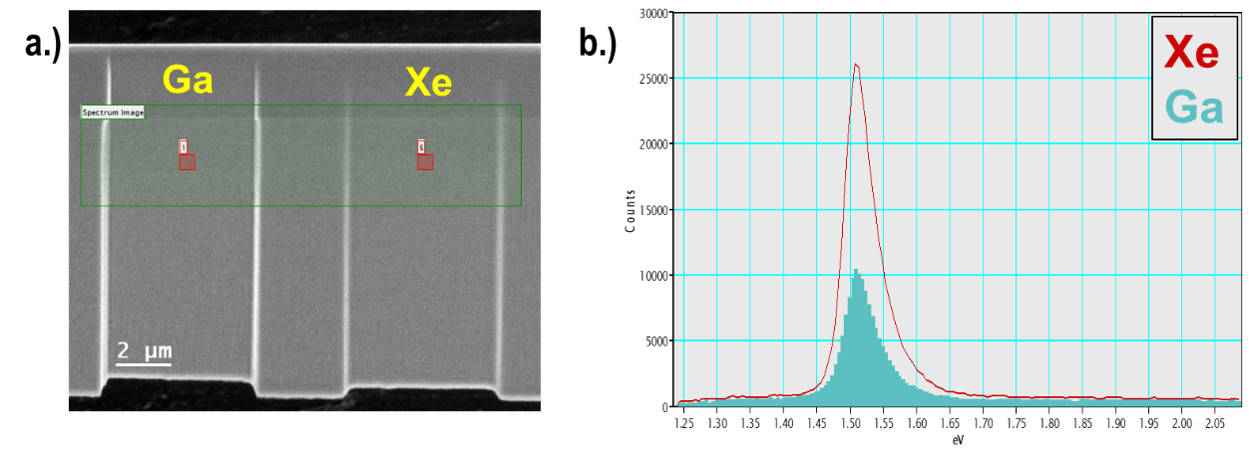
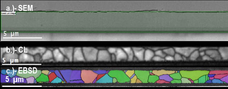
CdSeTe/CdTe devices were fabricated and cross-sectioned using Ga and Xe ion beams. The CL signal intensity from these regions was compared using a Monarc Pro CL detector. A novel CL-guided FIB lift-out workflow was developed, integrating CL, electron backscatter diffraction (EBSD), and backscattered electron (BSE) imaging to correlate SEM and TEM features.
Results
Xe ion-polished regions exhibited ~2.5 times higher CL intensity than Ga-polished areas, demonstrating superior signal preservation. CL and EBSD imaging provided detailed grain structure and luminescent property data, surpassing traditional secondary electron imaging. The optimized workflow reduced sample preparation time by eliminating redundant processing steps, such as Pt/W deposition.
Summary
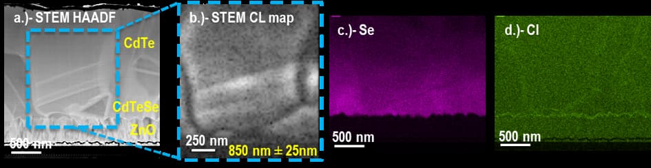
This study presents an efficient CL-guided workflow for TEM specimen preparation, enhancing microstructural characterization of solar cells. The integration of SEM, EBSD, EDX, CL, and STEM-CL techniques enables a comprehensive analysis from the micron to the atomic scale. Xe plasma FIB preserves CL signals more effectively, making it the preferred method for TEM-CL analysis. The approach improves resolution, minimizes damage, and streamlines sample preparation, advancing solar cell research.
Acknowledgement
Dr Stuart Robertson
Funding
The authors acknowledge access to the National Facility for High Resolution CL Analysis of Photovoltaic and Optoelectronic Devices, funded by the EPSRC (Grant No. EP/X030245/1).