Lithography
Lithography enables the printing of complex patterns on many different surfaces
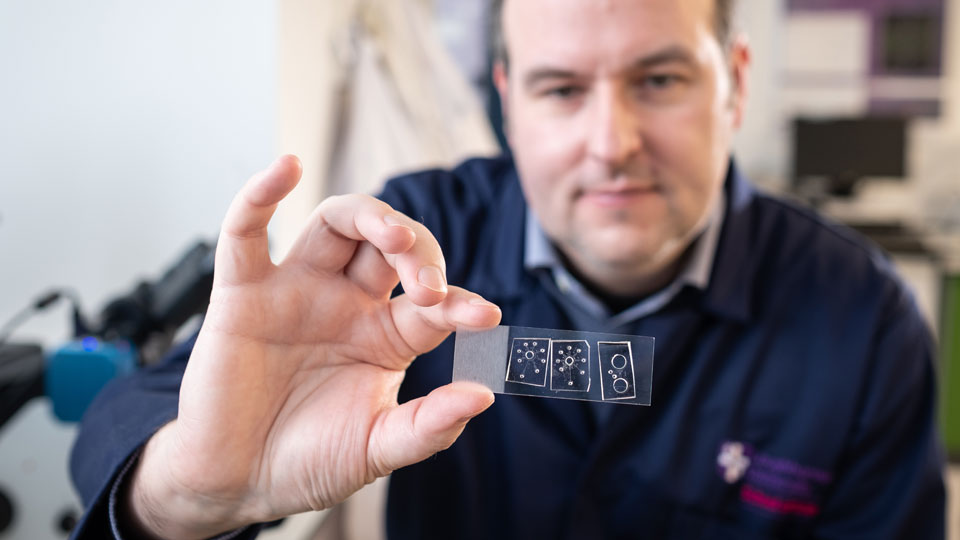
Optical and electron beam lithography techniques are used to create nano-patterned electronic devices – with features smaller than the size of a speck of dust.


Nature’s glow sticks
Many sea creatures and insects – including the firefly or glow worm – produce and radiate light through bioluminescence which occurs when chemical compounds mix together. Light is controlled in a particular pattern to attract mates and prey - and avoid predators. Large groups of fireflies can sometimes be seen flashing in unison.
Optical lithography and integrated circuits
Optical lithography (photolithography) involves the use of a photosensitive polymer - a laser or shadow mask can be used to ‘write’ a pattern. It is commonly used to make integrated circuits (ICs).
How are integrated circuits used?
The applications of integrated circuits include:
- Computers
- Mobile phones
- Televisions
- Memory devices
- Sensors in cameras
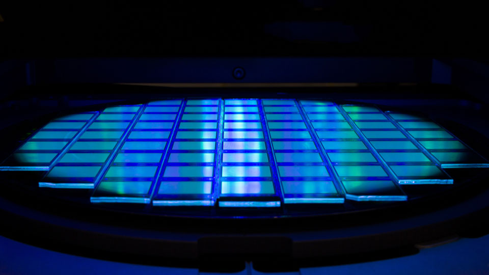
Brain-on-a-chip to revolutionise computing power
Loughborough scientists are exploring how neurons – the brain’s information processors – can be harnessed to supercharge computers’ ability to learn while dramatically cutting energy use. The Neu-ChiP project will layer networks of stem cells resembling the human cortex onto microchips and then stimulate the cells by firing changing patterns of light beams at them.
Related research at Loughborough
A variety of research areas benefit from greater control of light or the use of lithography.