National facility for high resolution cathodoluminescence (CL) analysis of photovoltaic and optoelectronic devices
Funded by the Engineering and Physical Sciences Research Council (£2.6M, EP/X030245/1), the National Facility for High Resolution Cathodoluminescence (CL) Analysis provides unique characterisation capability to maintain the UK's position as a research leader in photovoltaic and optoelectronic device development for the global energy transition. The facility has been supported by 14 universities and 11 companies ranging from raw materials suppliers, manufacturers to end users as partners.
Solar photovoltaics (PV) is the fastest growing form of renewable energy generation worldwide. The UK solar research community has established a global reputation for its work in PV research. Impact has included the discovery of new devices (perovskites, organic) as well as improvements in understanding and efficiency of silicon and thin film PV (CdTe and CIGS).
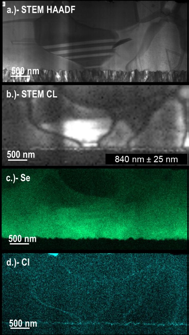
Advanced electronics and solar PV use progressively complex device structures. Device characterisation links detailed microstructural analysis with photoactivity to provide fundamental insights into the defects causing carrier recombination as well as mechanisms for their passivation. We pioneered the CL application to make breakthroughs in understanding why the addition of selenium improves the efficiency of thin film CdTe solar cells. Much more is being achieved by clustering a next generation CL capability on a SEM and a state-of-the-art TEM in conjunction with plasma-Xe focused ion beam specimen preparation (EPSRC multi-user call, EP/P030599/1).
Research aims
Our objective is to establish a unique and internationally leading facility for CL on scanning and transmission electron microscopes. The facility enables university and industrial researchers to correlate luminescence with defects, microstructure and composition down to the nanoscale.
The facility will comprise:
- CL on a dual beam Scanning Electron Microscope (SEM) equipped with a Xenon plasma Focused Ion Beam (FIB). The SEM-CL detector will enable large field-of-view characterisation from statistically relevant areas. Hence site-specific areas for STEM-CL analysis can be selected based on the CL emission and then prepared in-situ.
- CL on a dedicated Scanning Transmission Electron Microscope (STEM) for nanoscale analysis. STEM analysis combined with EDS provides detailed high resolution microstructural and elemental mapping and when combined with CL analysis, it provides correlations between defects and photoactivity which is crucial to improving device performance.
Methodology
The Facility is professionally managed and integrated into the well-established (20+ years) Loughborough Materials Characterisation Centre (LMCC), a multiuser core facility with dedicated instrument specialists that provides a well-supported environment to maximise the capacity of the equipment. LMCC supports the operation of the Facility and promote its use through a pump-prime scheme to generate early data and collaborations during the funded period up to January 2026. Beyond that the facility will run sustainably by collaborations on joint research grant as well as providing consultancy services to industry. Although PV devices are the application focus, the facility has included new detectors for research in LEDs, laser diodes, quantum dots, plasmonics, photonics and other optoelectronic device materials.
Findings
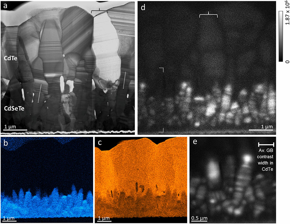
Instrumentation wise, new method has been developed. To maximize the combined advantages of SEM, EBSD, EDX, CL, STEM, STEM-EDX, and STEM-CL, an efficient workflow is essential for preparing samples from microstructural features of interest identified initially by SEM at the micron scale for detailed analysis in TEM down to the atomic scale. We have demonstrated an efficient focused ion beam (FIB) lift-out workflow that enables the preparation of TEM samples from site-specific photoactive areas identified using CL. This workflow enables significant time savings and precision in correlation between data sets.
The state-of-the-art TEM and CL have been applied to aid the record-breaking solar cell discovery. The use of SnO2 buffer layers has led to highly efficient and stable thin film CdSeTe/CdTe solar cells. However, chlorine segregation was observed at the SnO2/CdSeTe interface, suggesting that the quality of the p-n junction could be improved. ZnO has been incorporated between the SnO2 and
CdSeTe to study its passivation effect. The bilayer SnO2 (67 nm)/ZnO (30 nm) buffer layer has achieved an efficiency of 21.7% without an anti-reflection coating. High resolution TEM analysis showed atomically coherent boundaries at the SnO2/ZnO and ZnO/CdSeTe interfaces. The discovery that ZnO can be used as a passivation layer opens up new pathways to achieve highly efficient solar cells.
Both have been submitted to the 53rd IEEE Photovoltaic Specialists Conference June 8-13, 2025, Montreal.
Impact
Thin film CdTe is the most successful second-generation PV technology. High spatial resolution CL will also be a game changer in understanding the emitter/ absorber interface in highly doped CdTe solar cells containing a doped emitter. Combined TEM cross-section with bandgap mapping will enable better understanding of this critical interface and help engineer >25% efficient thin film solar cells.
References
- Fiducia, T.A.M., Mendis, B.G., Li, K. et al. Understanding the role of selenium in defect passivation for highly efficient selenium-alloyed cadmium telluride solar cells. Nat Energy 4, 504–511 (2019).
- Fiducia, T.A.M., Howkins, A., Abbas, A., et al. Selenium passivates grain boundaries in alloyed CdTe solar cells, Solar Energy Materials and Solar Cells, 238 (2022),111595, ISSN 0927-0248.
- Scarpulla, M.A., McCandless, B., Phillips, A. B., et al. CdTe-based thin film photovoltaics: Recent advances, current challenges and future prospects, Solar Energy Materials and Solar Cells, 255 (2023)112289,ISSN 0927-0248.
- Kornienko, V., Oklobia, O., Irvine, S., et al. Absorber texture and the efficiency of polycrystalline thin film CdTe solar cells, Thin Solid Films 793 (2024),140277,ISSN 0040-6090.
Experts involved
Staff:
- Prof Mike Walls (CREST)
- Prof Kelly Morrison (Physics)
- Dr Pooja Goddard (Chemistry)
- Dr Mike Jepson
- Dr Stuart Robertson
- Dr Ali Abbas
- Dr Zhaoxia Zhou
PhD researchers:
- Sam Machin
- Kieran Curson