Hot stage case study
In-situ thermal ageing of lead-free solder
Background
Cycling heating caused by sequential reflow soldering during the assembly of power modules can result in component damage and induces high residual stress due to Coefficient of Thermal Expansion (CTE) mismatches between power module layers. Self-Propagating Exothermic Reactions (SPERs) are a promising alternative to bonding large areas at quasi-ambient temperatures without the need for reflow soldering
The Intermetallic Compound (IMC) layer produced by SPER bonding is very thin, however, using P-FIB and hot stage heating the layer growth can be observed and quantified in real time. This technique offers an unprecedented opportunity to observe IMC growth.
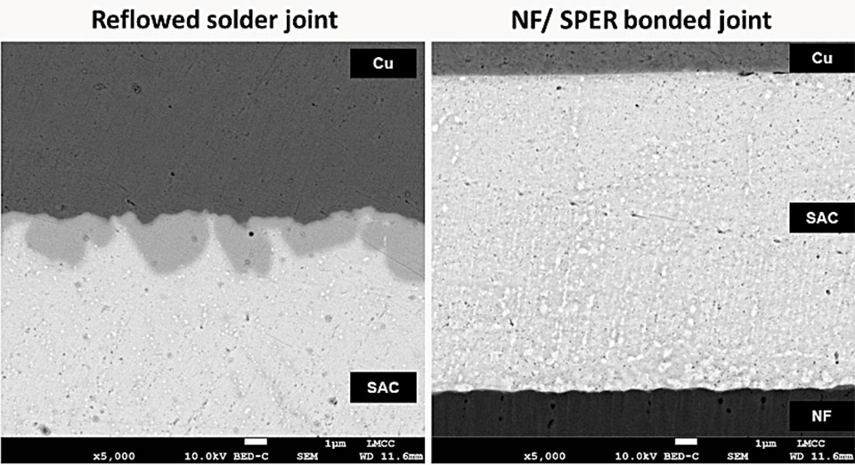
Comparison between conventional reflowed solder joint and a SPER bonded interconnect
Experimental
Using the Helios G4 P-FIB, (Thermo Fisher Scientific, USA) a layer of tungsten was deposited on the surface as Platinum readily alloys with tin. The sample was then cut with the Xe+ ion beam forming a lamellar 10 µm thick 120 µm long and 50 µm deep. The cutting and deposition steps shown in Fig 1 A-B:
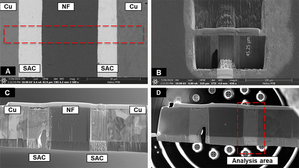
Once the sample was cut from the bulk it was transferred to the hot stage. The Micro-Electro-Mechanical Systems (MEMS) hot stage, on which the sample was attached, is capable of heating from 40°C to 1200 °C in both the SEM and TEM. The small mass of the chip allows for minimal drift and low inferred radiation, meaning high resolution imaging is achievable in the TEM and EDS and EBSD are possible in the SEM.
Cyclic heating was used to simulate thermal ageing. The sample was ramped from 50°C to 150 °C at 5°/min and held at 15-minute intervals for the first hour and 30-minute intervals for the following 2 hours. Backscatter images of the sample were continuously recorded; combined EDS and EBSD maps were recorded while the sample was at 50°C.
Results
IMC growth can be observed at both the copper and nano foil interfaces. EBSD was used to determine the IMC phase, whilst EDS and backscatter imaging was correlated with the EBSD data.
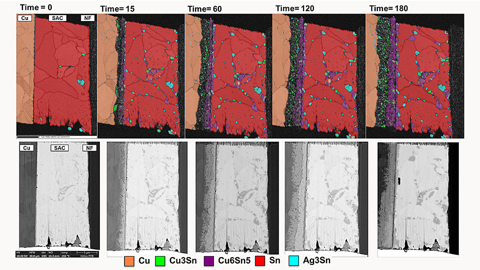
Cu6Sn5 was formed preferentially at the copper interface while a mix of Ag3Sn and Cu3Sn was formed at the NF interface.
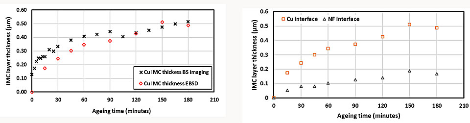
Back scatter image analysis matched well with the EBD results, estimating comparable IMC layer thickness at the copper interface. EBSD shows that the copper interface developed a thicker IMC layer than the NF layer. EBSD was also able to characterise the IMC type at each interface and the development of the grain size in the bulk of the sample.
Summary
In-situ thermal ageing can be used to monitor and understand IMC growth of solder joints. For SPER bonded samples, a thin IMC layer is initially formed. At the copper interface, this layer develops more than the IMC layer at the NanoFoil following ageing. The copper interface will likely be the weak interface following manufacture but this interface will strengthen over time until the IMC become too large. The modest IMC at the Nf interface are typically under less stress and develop slower.
Backscatter imaging and EBSD provided comparable information with regards to IMC thickness, however, EBSD provides additional information on phase and orientation. Due to the small area of analysis the statistical significance of these result is limited but this approach does provide incite as to how IMC’s form and their changing morphology over time.
Acknowledgement
Stuart Robertson
Funding
This research was supported by EPSRC (Grant No. EP/R032203/1) funding awarded to Professor Changqing Liu and Dr Zhaoxia Zhou. The authors acknowledge use of facilities within the Loughborough Materials Characterisation Centre and for access to the Helios PFIB, funded by the EPSRC grant EP/P030599/1.